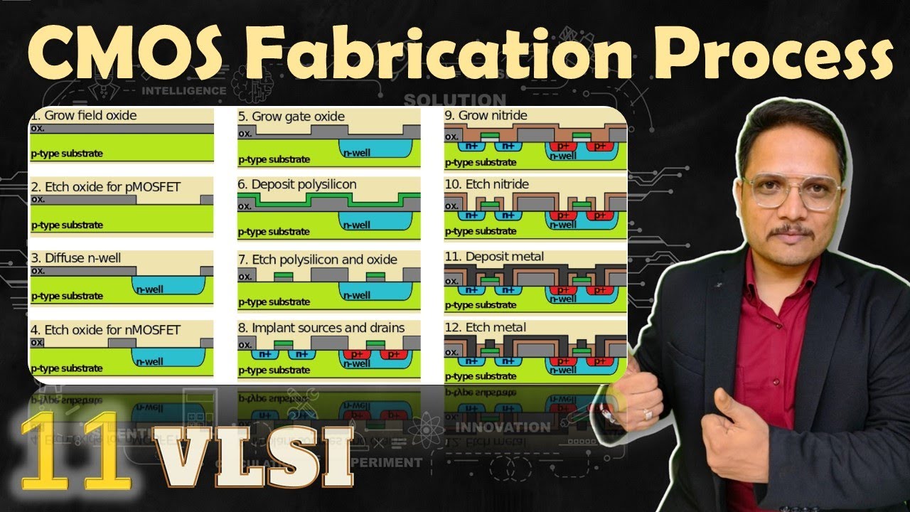
Solution: 12 cmos fabrication process 1 Cmos fabrication-n-well, p-well, twin tub process Cmos fabrication process
Lab
Chapter process fabrication vlsi systems Cmos fabrication using n-well and p-well technology Mosfet fabrication technology
Pmos transistor : cross section, working & its characteristics
Cmos fabrication (p-well process)Pmos fabrication steps with diagrams Download scientific diagramRepresentation of the working principle of a pmos transistor. the.
Nmos fabrication process principle explanationNmos fabrication process and steps with diagrams,silicon-gate process Design of vlsi systemsFabrication nmos ic process steps gate diagrams silicon techniques.

Cmos fabrication well pmos process nmos transistor using names assigning technology
Pmos transistor principle representation semiconductor一种改进型sic平面mosfet器件的制备方法与流程 Process flow of the main steps towards the fabrication of si (100) pmosCmos fabrication process.
Vlsi process fabrication chapter systems cmos technologyPmos fabrication vlsi Pmos fabrication process, pmos fabrication steps, vlsi design, pmosCmos fabrication ppt powerpoint presentation pmos nmos slideserve.
Fabrication mosfet mos technology nmos type steps devices sio layer constructed formation rfwireless
Nmos fabrication steps ppt presentationProcess fabrication flow nmos ic flowchart resister basic ppt powerpoint presentation lecture slideserve Fabrication cmos flow nmos vlsiNmos pmos symbols.
Introduction to nmos and pmos transistorsFabrication steps nmos ppt process vlsi cmos presentation Design of vlsi systemsCmos fabrication process.

Pmos transistor
Mosfet technologyNmos fabrication process steps Nmos transistor : cross section, working, circuit & its differencesPmos fabrication vlsi.
Pmos nmos structures mosfet structure mos fabrication cmos processCmos fabrication mbe sige representation Schematic representation of a cmos fabrication process with sige mbeSolved explain the fabrication steps of a pmos transistor.

Draw the nmos circuit as switch
20 steps of cmos fabrication processCmos fabrication Cmos fabrication process photoresist gate pmos ppt powerpoint presentation gnd drain source contact making.
.


NMOS Transistor : Cross Section, Working, Circuit & Its Differences

Schematic representation of a CMOS fabrication process with SiGe MBE

PMOS Transistor | Reversepcb

CMOS Fabrication-n-well, p-well, twin tub process - VLSI Design

CMOS FABRICATION (P-WELL PROCESS) | by Agnathavasi | Medium

PPT - CMOS Fabrication PowerPoint Presentation, free download - ID:9172433

NMOS Fabrication process and steps with diagrams,Silicon-gate process